GBC Power Troubleshooting
A bench workflow for a Game Boy Color that won’t turn on (or won’t stay on). Work through it in order: the checks are sorted so the most common faults — and the ones that need no soldering — come first. If your console powers on fine but misbehaves, use the GBC General Troubleshooting guide instead.
Everything here is based on Natalie the Nerd’s reverse-engineered CGB schematic and Nintendo’s CGB service manual, cross-checked against community bench measurements (sources at the bottom). Component designators are the stock CGB board’s.
What you need
- A multimeter with continuity beep and DC volts.
- Ideally a bench power supply with an adjustable current limit — the single most useful power-diagnosis tool. No bench supply? Fresh disposable AAs work for basic checks (not half-charged NiMH: 2.4 V starts you near the brown-out floor).
- IPA (90 %+), cotton swabs, and contact cleaner for the switch and terminals.
- Tri-wing driver to open the shell, Phillips for the board.
Safety first: never feed external power into the console while batteries are installed — alkaline cells can vent or explode if back-fed. And although this is a 3 V handheld, the powered board carries +13.6 V and about −15 V for the LCD around the DC-DC module and the screen ribbon, so probe deliberately.
How the GBC makes its power
Two AA cells (3 V nominal) or the DC jack feed one input rail; a boost/inverter module then generates everything else:
 DC jack P4 ── EM10 ── F2 ── EM7 ──┬── EM6 ── F1 ── SW1 ──► VCC (~3 V, switched)
                                   │                         │
 Battery BT+ ──────────────────────┤                   C31 (4.7 µF)
                                   │                         │
                             D2 (clamp to GND)          U5  DC-DC
                                                 ┌───────────┼────────┐
                                              +5 V       +13.6 V   −14.6 V
                                              (C32)       (C30)     (C22)
                                                 │           └── LCD ──┘
                                             U7 LDO
                                                 │
                                              +3.3 V (C39)
Worth knowing before you probe:
- Both inputs share one rail. The DC-jack path runs through its own fuse F2 (and the EM10/EM7 filters) and joins the rail right at the battery terminal node; from that node onward, both sources share EM6, fuse F1, and the power switch. D2 sits at the node as a reverse-polarity clamp to ground. The DC jack also contains a small normally-closed switch that physically disconnects the batteries when a plug is inserted — if that internal switch corrodes open, the console looks stone dead on batteries even though nothing else is wrong.
- VCC is just switched battery voltage. After SW1, the raw ~3 V rail (net
VCC) feeds the DC-DC converter U5 — and also directly feeds the audio amp U3, which is why a sagging battery rail shows up as audio trouble. - U5 generates three rails: +5 V (main logic and the cartridge), +13.6 V and a negative rail for the LCD bias. Nintendo’s manual calls the negative rail −15 V; Natalie’s schematic nets it as −14.6 V — expect a reading in that neighborhood. The LCD’s bias voltages are derived from it through zener D1 and a resistor network.
- U7 (a small LDO — commonly identified as a Ricoh RN5RT33A in service documentation; the reverse-engineered schematic leaves it unlabeled) drops the 5 V line to +3.3 V for the CPU’s 3.3 V domain, the work RAM, and the screen ribbon’s VDD3 logic supply. (The IR circuit runs from +5 V.) Its load is tiny (a few mA), so it rarely dies — but when it does, the console is “on” yet dead.
Expected voltages at each test point
Switch ON, fresh 3 V input, black probe on the BT− pad (the battery terminals are silkscreened BT+ / BT− on the board):
| Rail | Probe at | Expect | If missing, suspect |
|---|---|---|---|
| Battery input | BT+ pad | ~3 V (2.0 V is the design floor) | Cells, terminals, corrosion |
| Before switch | F1 output side | ~3 V | F1, D2 area, jack’s internal switch |
| VCC (switched) | C31 (4.7 µF) + side | ~3 V with switch ON | SW1 dirty/broken |
| +5 V | C32 (100 µF) + side | ≈ 5.0 V | U5 DC-DC, its solder joints |
| +3.3 V | C39 (1 µF) / U7 VOUT | ≈ 3.3 V | U7 regulator (needs 5 V first) |
| +13.6 V | C30 (1 µF) | ≈ +13.6 V | U5 (LCD-side output) |
| Negative LCD rail | C22 (1 µF) | ≈ −14.6 to −15 V | U5 (LCD-side output) |
Handy extra: pin 1 of the link port is on the +5 V rail, so you can sanity-check the boosted rail without even opening the shell.
The power switch is SPDT: in the OFF position it deliberately discharges the rail to ground through R1 (750 Ω). So roughly 750 Ω across VCC with the switch off is normal circuit behavior — but a near-0 Ω reading is still a real short.
Step 1 — Dead console: unpowered continuity checks
Batteries out, multimeter on continuity:
- Fuse F1 (shared path, after the sources merge) and fuse F2 (DC-jack path only): beep across each. A blown fuse is a dead-simple find. They’re ~1 A IC-protector types (
ICP-S1.0TNon the schematic; period repairs also cite 1.25 A Matsushita parts — anything in that class works). Never bridge a fuse permanently — it blew for a reason; find the reason, then fit a new fuse.- Useful tell: alive on batteries but dead on the adapter → F2 (or the jack-side filters). Dead on both with good cells and a clean switch → suspect F1, since it sits in the shared path. Dead on batteries but alive on the adapter is not a fuse — that points at the battery terminals or the jack’s internal switch.
- DC jack internal switch: with nothing plugged in, measure across jack pins 2 and 3 — you should read near 0 Ω. Open = the corroded-jack fault above. Bridging pins 2–3 is fine as a diagnostic, not as a fix.
- Power switch SW1: continuity from the common to the ON-side contact with the switch on, and none when off. Flaky or high resistance → clean it. IPA down the switch and working it back and forth helps; opening the switch and cleaning the contacts properly is the durable repair. A dirty SW1 is the single most common GBC power fault.
- Battery terminals: inspect for alkaline crust. Clean with IPA; use distilled vinegar for real corrosion (then rinse with IPA); replace terminals that are eaten through. Also check the cells actually reach the contacts — some aftermarket shells without the battery separator let them sit short.
Step 2 — Powered diagnosis with a bench supply
Set the supply to 3.0 V, current limit around 300 mA (the console is rated 3 V / 0.6 W ≈ 200 mA, and the OEM MGB-005 adapter was rated 300 mA). Batteries out, clip to the BT+ and BT− terminals following the silkscreen, switch the console on, and read the current meter — the draw is the diagnosis:
| Current at 3 V | Meaning |
|---|---|
| ~0 mA | Input path is open: blown F1, dirty SW1, corroded terminals, or the DC jack’s internal switch stuck open. Go back to Step 1. |
| Tens of mA up to ~150 mA, plays fine | Healthy. Published bench numbers vary (roughly 30–120 mA depending on game, cart type, and screen — flash carts and color games sit at the high end), but “well under the 200 mA rating” is the healthy zone. |
| Plausible current, but no picture | Power input side is fine — move to Step 3 and check the DC-DC outputs. |
| Several hundred mA / supply hits its limit | A short downstream: failed capacitor, damaged U5, or corrosion bridging traces. Unplug promptly and inspect around the DC-DC and the caps. |
Draw creeping up as you lower the voltage is normal (it’s a boost converter holding constant output power); the console is designed to run down to about 2 V.
Step 3 — Checking the DC-DC outputs
Console on and drawing plausible current, but dead or screenless? Probe the output side against the table above, in this order:
- +5 V at C32. Missing with a good ~3 V at C31 → the DC-DC module itself. Look first for cracked solder joints on U5 and reflow them — the module flexes with the board and this is a classic failure. If the joints are good and 5 V still won’t come up, replace the module (modern drop-in regulators exist from the usual suspects).
- +3.3 V at C39/U7. 5 V present but no 3.3 V → U7 has died (rare). Drop-in SOT-23-5 LDO replacements work.
- +13.6 V at C30 and ≈−14.6 V at C22. Both present but white/blank screen → the fault is past the power supply: ribbon seating at P2, then the display checks in the general guide. Either missing with a good 5 V → the LCD side of U5.
- Flicker, resets, dying audio, dim screen with all rails nominally present → aging electrolytic capacitors; recap kits target the power/audio/screen caps including C32.
CPU power pins
If every rail is good and it still won’t boot, verify supply is actually arriving at the CPU (CGB CPU, all revisions except E — pinout by Natalie the Nerd):
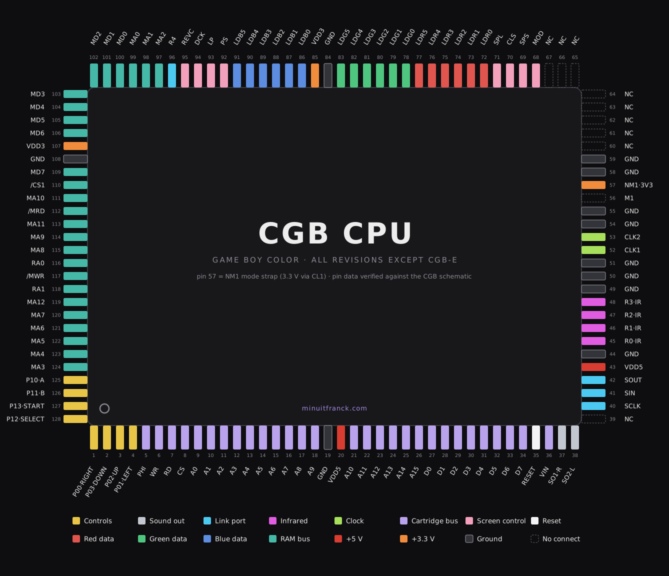
Our pinout reference (click for full size) — the supply pins are the red (+5 V) and orange (+3.3 V) legs; grounds are the dark outlined legs.
| Supply | CPU pins |
|---|---|
| +5 V | 20, 43 |
| +3.3 V | 85, 107 |
| GND | 19, 44, 49–51, 54, 55, 58, 59, 84, 108 |
| RESET (held by U6 PST9135N) | 35 |
(Pin 57 also reads 3.3 V on a working board, but it’s the NM1 mode strap tied to the rail through jumper CL1 — not a supply pin.)
No clock is a boot-killer too — see the “won’t boot” row of the CPU pin table in the general guide.
Sources & credits: CGB reverse-engineered schematic and CPU pinout by Natalie the Nerd; Nintendo CGB service manual (PDF, hosted at GameSX); bench current measurements by Jellybelly Customs (via Hand Held Legend); power-tracing notes from Hand Held Legend and Mouse Bite Labs; common-issues wisdom from the gbwiki.org / gameboy.github.io community docs; general methodology adapted from BucketMouse’s troubleshooting notes. Values like the −14.6 V vs −15 V negative rail differ between the service manual and modern measurements — I’ve noted both. This guide was researched and written with the help of Claude (Anthropic’s AI) — I’m a newbie working alone, piecing things together from trial and error, community Discords, Google, and YouTube, with AI helping me aggregate it all. Corrections welcome — email me.